An intuitive approach to operational principles of semiconductor devices. The course covers PN junction diodes, optical sensors, solar cells, LEDs, and Bipolar Junction Transistors. As a topic of study, semiconductor devices offer a unique challenge due to the complex mathematics involved. In this course, we take a more intuitive approach to explore the underlying concepts. Eschewing mathematics, we use engaging animations to help you visualize the working principles of many common semiconductor devices.
Class Deals by MOOC List - Click here and see EdX's Active Discounts, Deals, and Promo Codes.
Whether you are completely new to the subject or an experienced engineer, this course will give you a different perspective and a new way to look at the behaviors of semiconductor devices.
Reducing the reliance of equations does not mean the depth of the material is sacrificed. In fact, the course provides even more in-depth explanations of key concepts. We shift the focus from quantitatively evaluating the behavior of semiconductor devices to intuitively visualizing the semiconductor device actions.
In addition, the course offers a wide array of content - from basic PN junctions to modern nano-electronic circuit and systems. Besides covering the existing technologies, the course also explores the development of the industry into the future.
This course is part of the Principle of Semiconductor Devices Professional Certificate.
What you'll learn
- How to describe the motion of carriers in a semiconductor material
- Ways to illustrate the operational principles of some common electronic devices including PN Junction Diode, Schottky Diode, Photo Diodes, Solar Cells, LED and Bipolar Junction TransistorHow to identify the most important parameters to adjust for meeting certain design specifications
- How to construct the circuit models of some common electronic devices
- Communication in the language of semiconductor
Syllabus
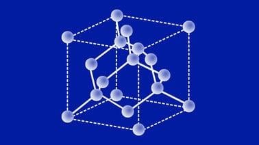
Week 1: Intrinsic semiconductor materials
Introduction to the energy band diagram of a crystal and calculating the carrier concentration in the material.
Week 2: Doping and PN junction formation
The effect of doping and the formation of PN junctions.
Week 3: Current-voltage characteristics of PN junction diodes
Current-voltage characteristics and detailed carrier actions in a PN junction diode.
Week 4: Real PN junction characteristics, its model and design
The characteristics of real PN junction diodes, the charge and capacitance models, and the design strategy.
Week 5: PN junction optical properties and metal-semiconductor contacts
The optical responses of the PN junction; the working principles of optical detection, solar cells and LEDs; and the metal-semiconductor contacts.
Week 6: Basic operation of Bipolar Junction Transistor
Introduction to bipolar junction transistors, I-V characteristic and non-ideal effects.
Week 7: Real Bipolar Junction Transistor structures, switching characteristics and model
Switching characteristics of the Bipolar Junction Transistor, it circuit model and design strategy.
Week 8: Final Exam