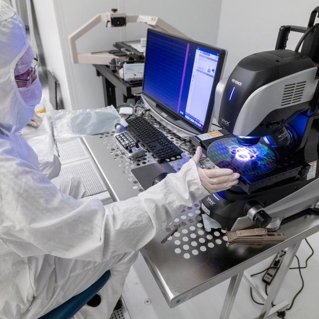
This course aims to provide a general understanding of semiconductor process. This course explores the principles and basic theory of semiconductor device and process. Furthermore, the students will learn the overall semiconductor process such as oxidation, diffusion, ion implantation, lithography, etching, thin film deposition, plasma, metallization, and packaging.
Class Deals by MOOC List - Click here and see Coursera's Active Discounts, Deals, and Promo Codes.
The lecture notes can be downloaded with registration, that helps students watch the videos. There are quiz problems to check your understanding of the lectures. To receive course certificate., you must score at least 60% of quiz within two chances.
Lecture notes, quiz and certificate are offered to registered students only.
Syllabus
Week 1 Wet Etch
Week 2 Plasma & Dry Etch
Week 3 Thin Film Deposition 1
Week 4 Thin Film Deposition 2
Week 5 Metallization, Chemical Mechanical Polishing, Strain Engineering
Week 6 Electronic Packaging
Week 7 Advanced Packaging 2.5D/3D
Week 8 DRAM Process
Week 9 3D Transistor Process