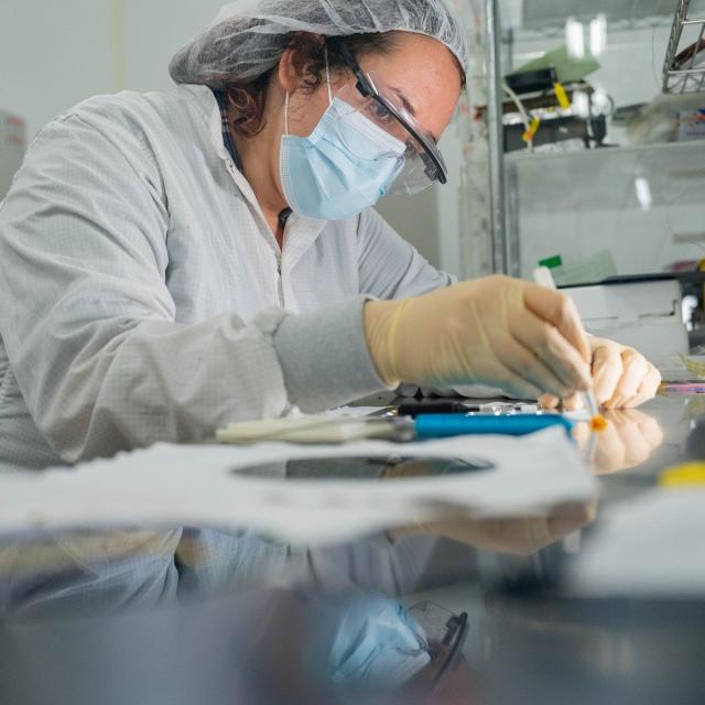
This course will cover various aspects of microelectronics and nanoelectronics. This field aims to advance and improve the functionality of electronic devices by scaling transistors to smaller feature sizes. The course will introduce you to essential concepts such as length scales, transistor actions, and feature sizes of integrated circuits.
Class Deals by MOOC List - Click here and see Coursera's Active Discounts, Deals, and Promo Codes.
The course will also look at historical observations and trends using Moore’s Law, which currently guides and predict development of the Semiconductor industry. Most importantly, our goal is to highlight why packaging is so important and relevant today. Furthermore, we will also explore the anatomy and function of a semiconductor package, starting with substrate-level package interconnection to the motherboard. We will also describe features as we differentiate various types of packages and how they differ in materials, design, and reliability.
Course 1 of 3 in the Semiconductor Packaging Specialization.
What You Will Learn
- Introduction to essential concepts such as length scales, transistor actions and feature sizes of integrated circuits.
- Historical observations and trends using Moores Law
- Explore the anatomy and function of semiconductor packaging.
- Recognize various types of packages and how they differ in materials, design and reliability.
Syllabus
WEEK 1
Welcome
Welcome to Introduction to Semiconductor Packaging. In this course, Dr. Terry Alford and Dr. Mitul Modi will share various aspects of microelectronics and nanoelectronics. This field aims to advance and improve the functionality of electronic devices by scaling transistors to smaller feature sizes. Our aim is to introduce you to essential concepts such as length scales, transistor actions, and feature sizes of integrated circuits. We also look at historical observations and trends using Moore’s Law, which currently guides and predict development of the Semiconductor industry. Most importantly, our goal is to highlight why packaging is so important and relevant today. Furthermore, we will also explore the anatomy and function of a semiconductor package, starting with substrate-level package interconnection to the motherboard. We will also describe features as we differentiate various types of packages and how they differ in materials, design, and reliability.
WEEK 2
Nanoelectronics
In this module, ASU Professor Terry Alford and Intel's Dr. Mitul Modi discuss nanoelectronics, a field that aims to advance and improve the functionality of electronic devices by scaling transistors to smaller feature sizes. Professor Alford and Dr. Mitul Modi will lead you through length scales, transistor actions, the great transistor, feature sizes, integrated circuits, Moore’s Law, and new markets. You will also learn about the new challenges for semiconductor packing that arise from nanoscale fabrication.
WEEK 3
What is Packaging? Part 1
In this module you will have an opportunity to view a lecture video by Principal Engineer, Dr. Mitul Modi from Intel as he discusses the challenges and opportunities in semiconductor packaging. He will explain why we package semiconductor die, describe the silicon to semiconductor package process flow, and how packaging is evolving to meet new market demands. He will also introduce the concept of heterogeneous integration, which enables higher functionality by combining different types of devices in a single package. You will learn how semiconductor packaging connects the silicon circuitry to the rest of the system, manages the power and signals, protects the silicon circuitry, enables cooling of the circuitry, and enables spanning many length scales.
WEEK 4
What is Packaging? Part 2
In this module you will have an opportunity to view a lecture video by Principal Engineer, Dr. Mitul Modi from Intel as he discusses Semiconductor Packaging; the past, present, and future. Mitul will explain the significance of Moore's Law, lead you through a condensed history of semiconductor packaging, and help you to identify the importance of packaging in the future, as well as why heterogeneous integration is important to the semiconductor industry.
WEEK 5
Anatomy of a Package Part 1
In this module you will have an opportunity to view a lecture video by Principal Engineer, Dr. Mitul Modi from Intel as he discusses the components and types of semiconductor packages. He will explain how the IC chip and the package substrate are connected by the flip chip interconnect (FLI) and how the package is connected to the motherboard by the second level interconnect (SLI). He will also describe other features that are added to some packages depending on the design, performance, and usage requirements. Mitul will also compare different types of packages and how they differ in materials, design, and reliability.
WEEK 6
Anatomy of a Package Part 2
In this module you will have an opportunity to view a lecture video by Principal Engineer, Dr. Mitul Modi from Intel as he discusses the structure and function of the package substrate in semiconductor packaging. He will describe the important features in the package substrate. Mitul will also discuss how the package substrate is designed for cost and performance trade-offs.
WEEK 7
Anatomy of a Package Part 3
In this module you will have an opportunity to view a lecture video by Principal Engineer, Dr. Mitul Modi from Intel as he discusses the mechanical, thermal, and electrical functions of semiconductor packaging. He will talk about how the package is used to manage environmental stresses, IC heat, power, and signals. He will also show how packaging involves different engineering skills and knowledge.
WEEK 8
Anatomy of a Package Part 4
In this module you will have an opportunity to view a lecture video by Principal Engineer, Dr. Mitul Modi from Intel as he discusses the reliability and customer ease of use. He will explain how the customer use of a package and the market use conditions affect the reliability need and the materials/design choices for the package. You will also learn how the importance of a common package footprint and second level interconnect (SLI) for motherboard design.
WEEK 9
Introduction to Semiconductor Packaging Course Summary
In conclusion of Introduction to Semiconductor Packaging, we would like to summarize the main takeaways. We started by sharing various aspects of nanoelectronics, transistor action, reliability, and customer ease of use. Then, we explored how Moore’s Law and market use conditions affect the packages' reliability needs and the materials/design choices. At the end, we saw how the common footprint of a motherboard or socket determines a package's substrate level interconnect. Thank you for joining us.