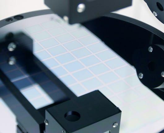
Electron and ion beams are widely used for both qualitative and quantitative analysis of semiconductor materials and devices. They can be used to image structures with sub-nm resolution and to provide information about elemental composition and dopant concentration. This course describes the fundamentals of electron and ion beam characterization and includes a project that analyzes the surface roughness of a solar cell.
Class Deals by MOOC List - Click here and see Coursera's Active Discounts, Deals, and Promo Codes.
This course is part of the Semiconductor Characterization Specialization.
What you'll learn
- Explain the interaction of electron and ion beams with semiconductor materials.
- Describe the constituent components of electron and ion beam characterization systems.
- Describe applications of electron and ion beam characterization.
Syllabus
Course Introduction
Electron and ion beams are widely used for both qualitative and quantitative analysis of semiconductor materials and devices. They can be used to image structures with sub-nm resolution and to provide information about elemental composition and dopant concentration. This course describes the fundamentals of electron and ion beam characterization and includes a project that analyzes the surface roughness of a solar cell.
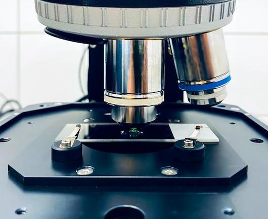
Week 4.1: Scanning Electron Microscopy
This week introduces the concepts of scanning electron microscopy and how it is used for both qualitative and quantitative sample analysis.
Week 4.2: Auger Electron Spectroscopy
This week, you will learn about Auger electron emission spectroscopy, a powerful technique for surface analysis.
Week 4.3: Secondary Ion Mass Spectroscopy
This week, you will learn about secondary ion mass spectroscopy and how it is used to measure the concentration and distribution of constituent materials in semiconductors.
Week 4.4: Course Wrap-up and Project
This week, you will complete a case study to assess your ability to use images obtained from an SEM for quantitative surface analysis.